Momentum is building up in semiconductor ecosystem in India, new plants in Odisha, Punjab and AP
The Union Cabinet chaired by PM Narendra Modi approved four more semiconductor projects under India Semiconductor Mission (ISM).
Momentum is building up in semiconductor ecosystem in India with the six approved projects already in various stages of execution. These four proposals approved on Tuesday are from SiCSem, Continental Device India Private Limited (CDIL), 3D Glass Solutions Inc., and Advanced System in Package (ASIP) Technologies.
These four approved proposals will set up semiconductor manufacturing facilities with cumulative investment of around Rs.4,600 crore and are expected to generate a cumulative employment for 2,034 skilled professionals which would catalyse the electronic manufacturing ecosystem resulting in creation of many indirect jobs. With these four more approvals today, total approved projects under ISM reaches to 10 with cumulative investments of around Rs.1.60 lakh crore in six states.
Given the growing demand of semiconductors in telecom, automotive, datacentres, consumer electronics and industrial electronics, these four new approved semiconductors projects would significantly contribute to making Atmanirbhar Bharat.
SiCSem and 3D Glass will be set up in Odisha. CDIL is located in Punjab and ASIP will be set up in Andhra Pradesh.
SicSem Private Limited is collaborating with Clas-SiC Wafer Fab Ltd., UK, to establish integrated facility of Silicon Carbide (SiC) based Compound Semiconductors in Info Valley, Bhubaneshwar, Odisha. This will be 1st commercial compound fab in the country. The project proposes to manufacture Silicon Carbide devices. This compound semiconductor fab will have an annual capacity of 60,000 wafers and packaging capacity of 96 million units. The proposed products will have applications in Missiles, Defence equipment, Electric Vehicles (EVs), Railway, Fast Chargers, Data Centre racks, Consumer Appliances, and Solar Power Inverters.
3D Glass Solutions Inc. (3DGS) will be setting up a vertically integrated advanced packaging and embedded glass substrate unit in Info Valley, Bhubaneshwar, Odisha. This unit will bring world’s most advanced packaging technology to India. Advanced packaging brings the next generation of efficiency to semiconductor industry. The facility will have a large variety of advanced technologies including glass interposers with passives and silicon bridges, and 3D Heterogeneous Integration (3DHI) modules. Planned capacity of this unit will be approximately 69,600 glass panel substrates, 50 million assembled units, and 13,200 3DHI modules per annum. The proposed products will have significant applications in defence, high-performance computing, artificial intelligence, RF and automotive, photonics and co-packaged optics etc.
Advanced System in Package Technologies (ASIP) will setup a semiconductor manufacturing unit in Andhra Pradesh, under technology tie-up with APACT Co. Ltd, South Korea, with an annual capacity of 96 Million units. The manufactured products will find applications in mobile phones, set-top boxes, automobile applications, and other electronic products.
Continental Device (CDIL) will expand its discrete semiconductor manufacturing facility at Mohali, Punjab. The proposed facility will manufacture high-power discrete semiconductor devices such as MOSFETs, IGBTs, Schottky Bypass Diodes, and transistors, both in Silicon and Silicon Carbide. The annual capacity of this brownfield expansion will be to the tune of 158.38 million units. The devices manufactured by these proposed units will have applications in Automotive electronics including EVs and its charging infrastructure, Renewable energy systems, Power conversion applications, industrial applications and communication infrastructure.
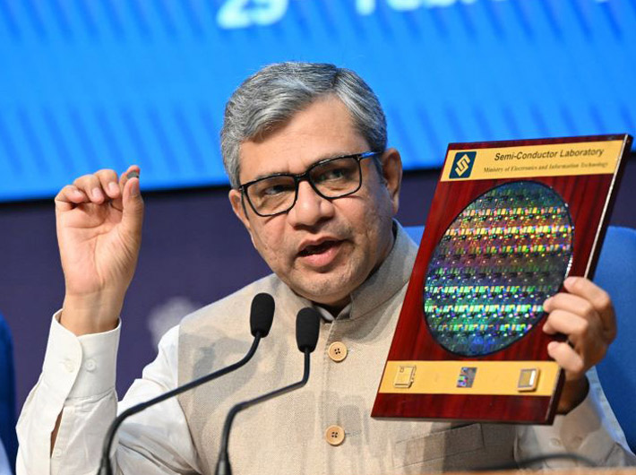
With the approval of these projects, semiconductor ecosystem in country would get significant boost as these projects include country’s first commercial compound fab as well as highly advanced glass-based substrate semiconductor packaging unit.
These would complement the growing world class chip design capabilities coming up in the country which are propelled by design infrastructure support provided by Government to 278 academic institutions and 72 start-ups.
More than 60,000 students have already availed the benefits of talent development programme.